It seems that there is an error in the original schematic, or I miss one inversion (sorry for that).
I did not check the schematic, so don't take my silence as a sign that it is OK. Actually, I do not understand why this circuit is configured that way at all, i.e.: a 230V, 15A BJT being driven by several MOSFETs. Why not use one high-power N-ch MOSFET being driven by a specialized gate driver (e.g. the UCC27511), like it is done usually? Also, I do not understand why the low/high side driver (IR2113) appears to drive two N-Channel MOSFETd (Q3 & Q4) which have their both sources grounded. Alas, the entire purpose of a high-side driver is to drive the gate of an N-channel MOSFET, which typically has its source connected to a high voltage rail ( i.e.: not grounded ! ) in order to completely avoid using a P-channel MOSFET (like the Q5 *). The high half of the IR2113 driver simply: 1) connects the HO output to the VB input when the the HIN input is high (and SD input is low). 2) connects the HO output to the VS input when the the HIN input is low (or SD input is high). ...while the VS and VB inputs are at voltage levels which are typically well ABOVE ground (also VB > VS+8.6V )**.Below is a diagram of this typical connection from the IR2113's datasheet: 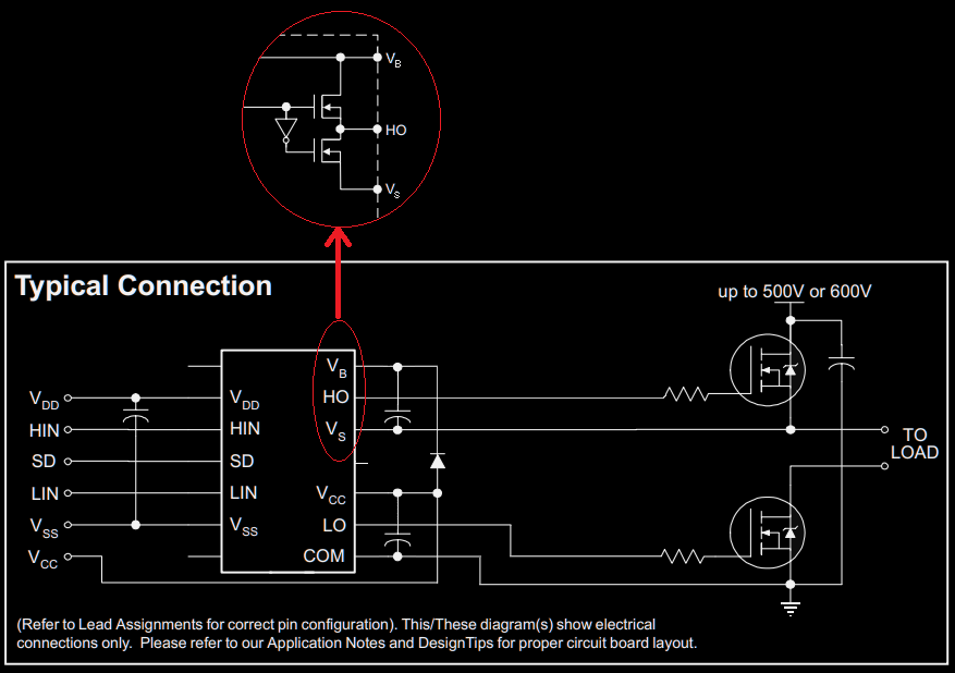 The only advantage of the IR2113 driver (which are two drivers in one package: a low-side driver and high-side driver) over the UCC27511 driver, is its duality and the ability to pull up and pull down the load solely with N-ch MOSFETs, while an N-ch MOSFET driven by the single UCC27511 driver can only pull down the load. By connecting together the COM and VS pins of the IR2113, that "push-pull" advantage solely with N-ch MOSFETs, is nullified. * this also makes the blocking diode on its drain unnecessary (re.: SR510).
** which is why I wanted to see these voltage levels simultaneously on both output pins.
« Last Edit: 2021-05-09, 20:53:57 by verpies »
|

 Author
Topic: Dally, Shark & Ruslan workbench (Read 223453 times)
Author
Topic: Dally, Shark & Ruslan workbench (Read 223453 times)
